
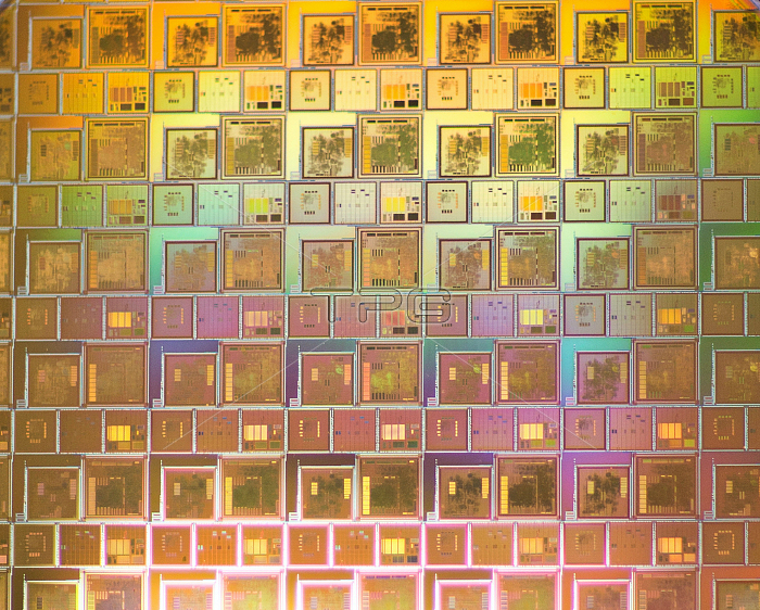
This 20 cm-diameter silicon wafer is etched with 35 replicas of five different chips for various space agency missions, each one incorporating up to about 10 million transistors or basic circuit switches. Laid down within a microchip, these designs endow a space mission with intelligence, and the ability to perform various specialized tasks such as data handling, communications processing or attitude control. To save money on the high cost of fabrication, various chips designed by different companies and destined for multiple European Space Agency projects are crammed onto the same silicon wafers, etched into place at semiconductor manufacturing plants. Once tested for functionality, the chips on the wafer are chopped up and packaged for use, then mounted on printed circuit boards for connection with other microelectronic components aboard a satellite.
| px | px | dpi | = | cm | x | cm | = | MB |
Details
Creative#:
TOP22300105
Source:
達志影像
Authorization Type:
RM
Release Information:
須由TPG 完整授權
Model Release:
N/A
Property Release:
No
Right to Privacy:
No
Same folder images:
 Loading