
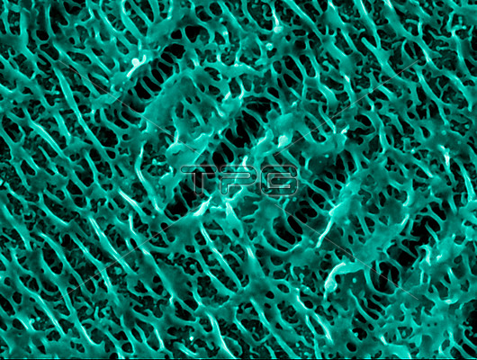
Nanowires on nickel. Coloured scanning electron micrograph (SEM) of nanowire structures formed on a nickel surface by pulses of a laser beam. This research involves the use of lasers to etch and ablate metal and semiconductor surfaces. The resulting nanostructures can have applications in various forms of electronics and nanotechnology.
| px | px | dpi | = | cm | x | cm | = | MB |
Details
Creative#:
TPG34696075
Source:
達志影像
Authorization Type:
RF
Release Information:
須由TPG 完整授權
Model Release:
N/A
Property Release:
N/A
Right to Privacy:
No
Same folder images:
 Loading