
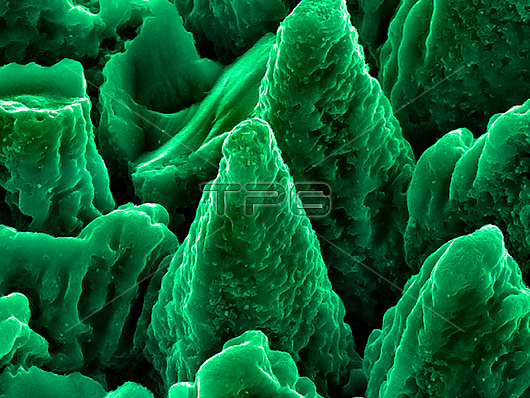
Microcones on silicon. Coloured scanning electron micrograph (SEM) of microcones formed on a silicon surface by a laser beam. This research involves the use of lasers to etch and ablate metal and semiconductor surfaces. The resulting microstructures and nanostructures can have applications in various forms of electronics and nanotechnology.
| px | px | dpi | = | cm | x | cm | = | MB |
Details
Creative#:
TPG34696089
Source:
達志影像
Authorization Type:
RF
Release Information:
須由TPG 完整授權
Model Release:
N/A
Property Release:
N/A
Right to Privacy:
No
Same folder images:
 Loading